This application report presents three measurement approaches for vibration analysis of printed circuit boards using Optomet laser Doppler vibrometers.
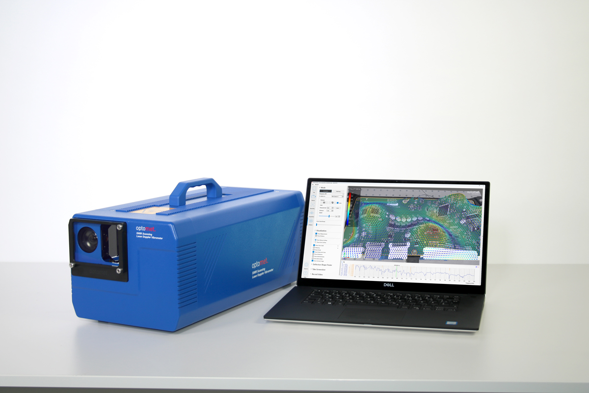
Full-area out-of-plane measurement: A single scanning vibrometer captures the vibration component normal to the board surface. Six steps from setup to component detail analysis demonstrate the complete workflow. The results identify spatial vibration hotspots, reveal mode shapes at board level and show the individual vibration behavior of single components.
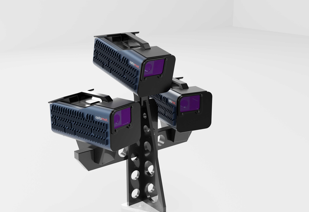
3D vibration analysis: Three synchronized SMART Scan+ vibrometers capture the complete motion in X, Y and Z. This reveals lateral movement, tilting motion and coupled modes that remain hidden in the out-of-plane measurement. The same system also captures thermal expansion – relevant for assessing thermo-mechanical reliability.
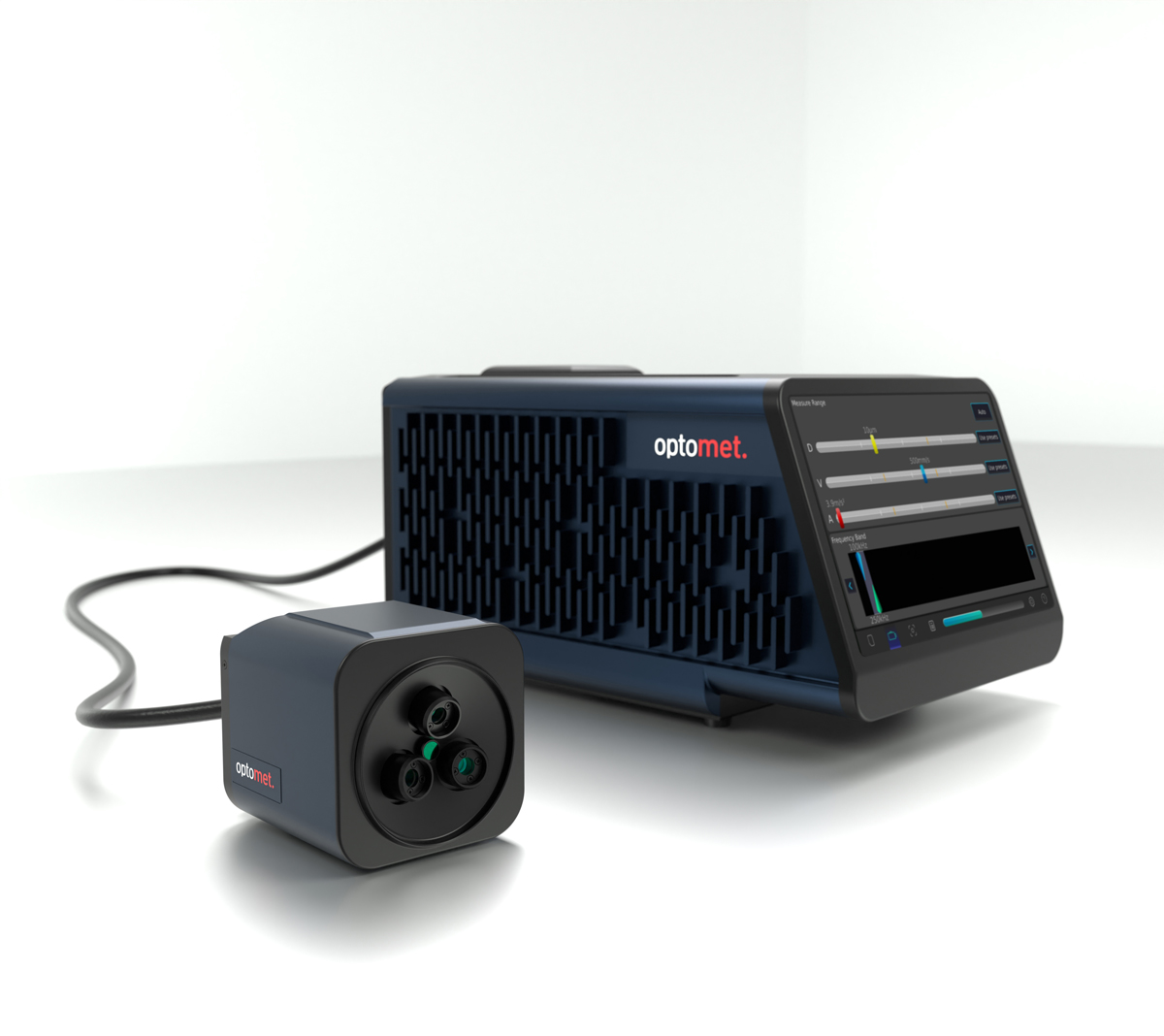
3D single-point measurement: The SMART 3D-Fiber provides complete 3D vibration information at a defined measurement point. The compact fiber-optic sensor head is suited for shaker tests on electronic control units, component qualification and integration into existing test rigs.
All three approaches deliver the spatial evidence for targeted design decisions: component repositioning, local stiffening, adjustment of mounting conditions or FEM validation against measured reality.
 SMART Scan+
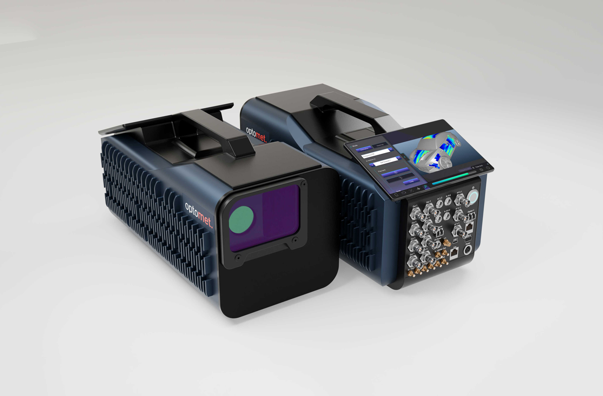
 SMART 3D-Scan
 SMART Full Body
 SMART Single+
 SMART Multi-Fiber
 SMART 3D-Fiber
 SMART DAQ
 Software SMART Lab
 Scanning Vibrometer
 Vector-Series
 Vector-Micro-Optics
 Nova-Series
 Nova-Xtra
 Fiber-Series
 Fiber-Multiplex
 Fiber Micro Manipulator
 OptoSCAN
 OptoGUI
 Single-Point Vibrometers
 Scanning Vibrometers
 3D-Laser Vibrometers
 Acoustics & Ultrasonics
 Aerospace and aviation
 Automotive
 Biology & Medicine
 Brake noise
 Civil Engineering
 Electronics & Household Devices
 Materials Research
 Medical technology
 Tools & Machinery
 Turbine
 Wind tunnel testing